COINFLIP Project: Coupled Organic-Inorganic Nanostructures for Fast, Light-Induced Data Processing.
The main objective of this project is to design optical switches with a response time < 5 ps, a switching energy < 1 fJ/bit and compatibility with silicon technology to excel in high-speed data processing at low heat dissipation. This will be pursued by combining the chemistry of inorganic, nanocrystalline colloids and organic semiconductor molecules to fabricate thin films of organic-inorganic hybrid nanostructures (Figure 1).
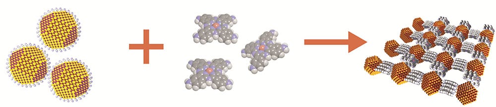
Figure 1. Modular design of coupled organic-inorganic nanostructures.
Optical switches play a pivotal role in modern data processing based on silicon photonics, where they control the interface between photonic optical fibers used for data transmission and electronic processing units for computing. Data transfer across this interface is slow compared to that in optical interconnects and high-speed silicon transistors, such that faster optical switching accelerates the overall speed of data processing of the system as a whole.
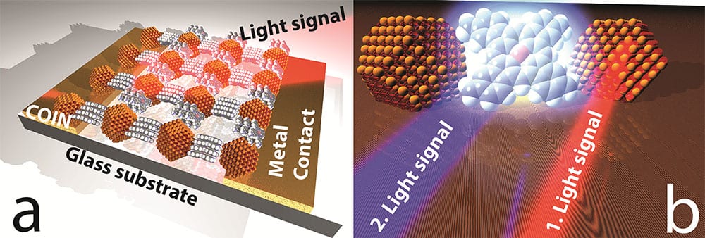
Figure 2. Scheme of an optical switch with activated absorption.
By modifying the surface of the inorganic nanocrystals with conductive molecular linkers and self-assembly into macroscopic solid state materials, new electronic and photonic properties arise due to charge transfer at the organic/inorganic interface. The multiple optical resonances in these hybrid materials result in strong optoelectronic interactions with external light beams, which are exploited for converting photonic into electronic signals at unprecedented speed (Figure 2a). A key concept here is an activated absorption mechanism, in which the nanocrystals act as sensitizers with short-lived excited states, which are activated by a first optical pump beam. Efficient charge transfer at the organic/inorganic interface temporarily creates additional resonances in the molecular linkers, which may be probed by a second optical beam for as long as the sensitizer is in its excited state (Figure 2b). Utilizing nanocrystals with excited state lifetimes < 5ps will reward ultrafast response times to pave the way for novel optical switches and high-speed data processing rates for silicon photonics.
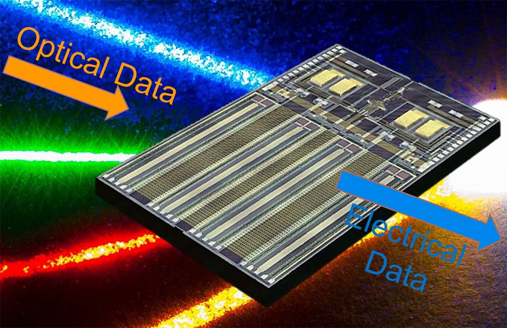
Figure 3. Scheme of an optical transceiver to convert optical into electric data.
Mid-term impact of the project on information technology.
Optical switches are ubiquitous in information technology due to the inevitable need to process photonic signals transmitted by optical fibers into electronic information for complementary metal oxide semiconductor (CMOS) chips (Figure 3). With data communication via optical fibers close to the speed of light and transistor switching speeds in the high GHz regime, the optical/electric interface is by far the slowest component of current data processing units. Optical switches with faster data transmission will therefore have a direct impact on current silicon photonics technology, in particular if the material is compatible with CMOS technology.
Anticipated long-term effects.
State-of-the-art, commercially available central processing units (CPU) operate at a clock rate < 5 GHz. While the precise relationship is complex, such processors require switching speeds of approx. 20 ps per individual, constituting transistor. To achieve this switching velocity with classical transistor technology, very small gate dimensions (~14 nm) are required with exceptionally thin dielectric layers. This is accompanied by higher parasitic leakage currents through the dielectric, leading to a larger power consumption of every transistor. Thus, although higher switching speeds are already possible, their implementation in CPUs is impractical due to the large power densities they would incur. For reference, typical CPUs operate with a thermal design power of ~150 W, which – depending on the precise CPU dimensions – translates into a power density of ~30 Wcm-1 or several times the power density of a typical hot plate. Thus, although the implementation of optical switches instead of field-effect transistors into CPUs requires substantial further technological breakthroughs in terms of the light sources, this development may become feasible in the long-term. This has the potential to break the current barrier in CPU clock speed, which is not only due to limited switching speeds but also because of the exponential increase in heat dissipation. Given that clock speeds have stagnated since 2003 for this reason, overcoming this barrier would signify a major leap for information technology. The materials and devices developed during the present project will provide important building blocks for such a high-speed data processing technology.