Carbon nanotubes
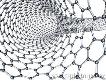
Properties of carbon nanotubes Carbon nanotubes (CNTs) are rolled up graphene sheets. Depending on the roll-up vector of the hexagonal sheet, CNTs are either semiconducting or conducting. |
Schematics of a CNT (ref.: sciencephoto.com) |
Low temperature growth of CNTs Because of their high inner surface, CNTs are well suited as electrode materials. Their optimal growing temperature is around 700 °C, which for many insulating, flexible materials, like polymers, is too high. Materials that are not damaged by such temperatures are ceramics or quartz glass, which however are brittle and inflexible. |
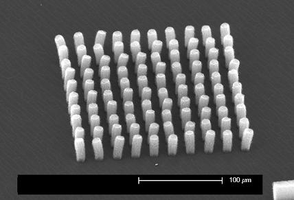
CNT bundles on a structured substrate |
CNTs as electrode material for neuronal applications Due to their good electrochemical properties, chemical inertness, and high inner surface, CNT electrodes are suitable for long term recording and stimulation of electrical cell activity and measurement of biochemical quantities. |
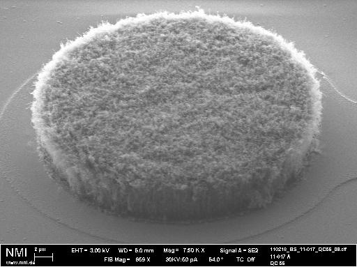
CNT electrode, 30 μm in diameter |
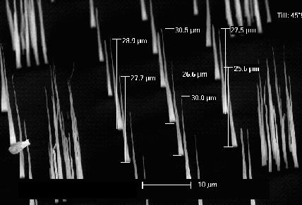
Carbon nanofibers for the detection of atoms Freestanding, vertically aligned multiwalled CNTs can be obtained in a plasma enhanced CVD process (PECVD-process). Their high aspect ratio leads to field enhancement at the tips, which makes it possible to ionize atoms and subsequently detect them. An arrangement of nanofibers allows for the investigation of their interactions with ultracold atoms. In order to achieve multiwalled CNTs with the required height and sharpness for this purpose, suitable growth processes are researched. |
Free-standing multiwalled CNTs |
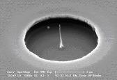
CNT as electron emission source In this application the high aspect ratio of carbon nanotubes is taken advantage of. The aim is to produce a miniaturized electron source which is completely integrated with a chip. Because of the high aspect ratio, a high electric field is created at the tip of the CNT. This way it is possible to obtain free electrons by field emission with a low voltage (some 10 V). |
CNT field emitter and electrode |
CNT transistors The aim of this project is the fabrication of n- and p-type transistors using a CNT as the conducting channel that exhibit characteristics which are comparable with or surpass those of current silicon MOSFETs. The CVD growth of the CNTs occurs directly on the substrate. In order to control the growth direction, they are grown in an electrical field aligned parallel to the substrate, which is applied by microelectrodes structured on the sample. |
Design for a CNT transistor |