Surface Imaging
HIM | SEM | FIB | optical microscopes
HIM - Helium Ion Microscope
The helium ion microscope provides excellent resolution in imaging combined with a very high depth of field. The helium ions are produced at a tip of only three individual atoms, the trimer. Each of these atoms generates an ion beam in the helium atmosphere at the tip. The most intensive beam is selected and directed into the microscope's optics and focused on the sample. Helium ions penetrate much further into the substrate than electrons at the same acceleration voltage. As a result, the beam mainly widens at depths from which secondary electrons can no longer escape the substrate. In this way, even better resolution can be achieved than with an electron microscope.
Zeiss ORION Nanofab
The Orion Nanofab provides a maximum resolution of 0.4 nm at a depth of field that is 5-10 times greater than a scanning electron microscope. Secondary electrons are used for imaging as standard, whereby only SE from the top few nanometers of a surface contribute significantly to the signal. As a result, the HIM offers an extremely high surface sensitivity and is able to image layers with the highest resolution, which would only be visible in the SEM at very low acceleration voltages due to the penetration lenght of electrons.
Since substrates are always positively charged by helium ion bombardment, they can be neutralized in the HIM with an electron floodgun. The HIM is therefore particularly suitable for imaging insulating substrates.
The Orion Nanofab also has two Kleindiek manipulators that can be used, for example, to position nanoparticles or to contact individual electrodes.
In addition, the gas injection system with three precursors can also be used to selectively deposit platinum, tungsten or silicon oxide containing layers (see ion-beam-induced deposition).

SEM - Scanning Electron Microscope
In an electron microscope, a focused electron beam is scanned line by line over a substrate. At each position of the electron beam, the interaction with the substrate generates a signal whose intensity is represented by the brightness on a gray scale. Each scan produces a black-and-white image of the surface containing information about the topography and possible differences in material.
The secondary electrons (SE) created by inelastic scattering are mainly used to map the surface. SE have a very low energy of approx. 5 eV (by definition < 50 eV), whereby mainly SE from the uppermost 1-10 nm of the surface contribute to the signal and enable the high resolution of a SEM. The SE are typically detected by an Everhart-Thornly detector. Since the ET detector is located sideways of the column, the topography has a significant influence on the signal by shading the side walls (dark areas) away from the detector and an increased SE yield on inclined surfaces (bright areas).
Alternatively, backscattering electrons (RE) can also be used to depict the surface. Electrons of the primary beam, which are elastically reflected in the material and leave the substrate with almost undiminished energy, are called RE. The illustration with RE can above all produce a very good material contrast, since its yield depends linearly on the atomic number of the element. RE are virtually unaffected by the comparatively low suction voltage of the ET detector. A separate detector is therefore used for detection, whose segments cover the largest possible angle range above the substrate for signal optimization. If the signal of the different segments are added, the topography influence is minimized and one gets a quasi pure material contrast image. If, on the other hand, the signal of opposing segments is subtracted, the topography contrast is maximized.
JEOL JSM-6500F
Our JSM-6500F is a field emission SEM with a Schottky field emitter. The column allows operation with acceleration voltages of 0.5 kV - 30 kV and offers a maximum resolution of 2 nm in the range of 5 - 30 kV. The stage accepts samples up to 2" diameter and 30 mm height and allows a tilt of up to 70°. The system is equipped with a retractable backscatter electron detector.
In addition, EDX and EBSD detectors allow the analysis and mapping of chemical and crystallographic composition.
ZEISS LEO Gemini 1550 VP
Our LEO 1550 VP is a field emission SEM with a Schottky field emitter. The column allows operation with acceleration voltages of 0.2 kV - 30 kV and offers a max. resolution of 5 nm in the range of 1 - 30 kV. The stage accepts samples up to 2" diameter and 30 mm height and allows a tilt of up to 90°.
The SEM also offers two Kleindiek manipulators (MM3A-EM), which can be used, for example, to position nanoparticles or make precise contact with electrodes. A micro-gripper (MGS2-EM) and a gas injection system (GIS-EM) are also available as extended accessories.
FIB - Focused Ion Beam
An FIB works principally similar to a scanning electron microscope, with the difference of typically gallium ions being focused into a beam instead of electrons. The gallium ions are obtained from a liquid metal ion source whose lifetime is limited by the consumption of the Ga supply. Since Ga ions have a multiple of the mass of an electron and are typically also accelerated to 30kV, the energy input into the substrate is significantly higher, so that the surface atoms of the substrate are removed. With the gallium beam it is possible to create structures with a resolution of up to 30 nm.
FEI Strata DB235
The Strata DB235 is a dual beam system, i. e. it has an electron column for imaging in addition to the Ga-column. The columns are mounted at an angle of 52° to each other.
The electron column has an Everhart-Thornly detector for imaging in standard mode and an additional through-lense detector for ultra-high resolution mode. The column offers a maximum resolution of 1.8 nm in UHR mode.
The ion column is mainly used for processing substrates (cross sections, TEM lamellae, nano structuring), but can also be used for imaging. Particularly interesting is the use of the ion beam for the visualization of grain boundaries and their orientation. The material contrast can also be enhanced by imaging with secondary ions compared to the electron beam. A CDM-E/-I detector is available for the ion column, which offers an optimized S/N ratio for the ion beam.
The Strata DB235 can take samples of up to 2" in diameter and approx. 10 mm in height.
Unfortunately, our system is out of order, but we will happily give advice on alternative systems from our colleagues at other institutes.
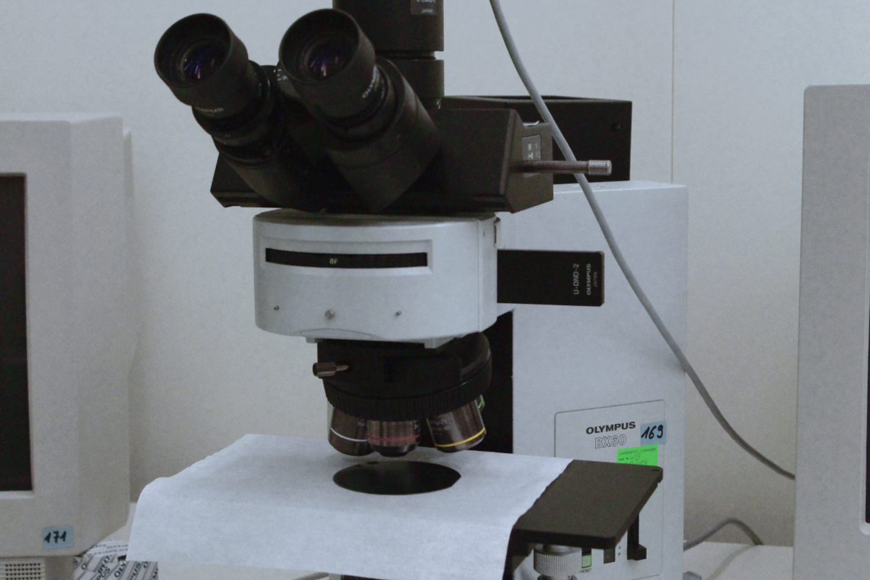
Optical Microscopes
The two Olympus MX50 and BX60 inspection microscopes are available to LISA+ users in our clean room:
Olympus MX50
The MX50 is located in the photolithography laboratory and is equipped with a Differential Interference Contrast (DIC) module and a red filter, e. g. for the inspection of lithographically created photoresist structures. The microscope can be operated in reflection or transmission mode. A Leica EC3 digital camera is available for documentation. The UIS lenses offer magnifications of 5x, 10x, 20x, 50x, and 100x with an additional 10x magnification through the eyepiece.